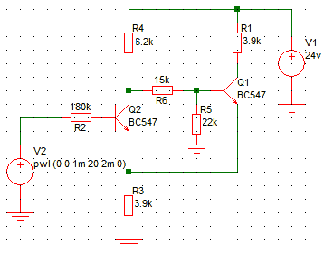
This article shows how to design a Schmitt trigger using transistors, how to improve the basic design, and why it might sometimes be the best approach.
What does it do?
A Schmitt trigger is a decision-making circuit. It is used to convert a slowly varying analogue signal voltage into one of two possible binary states, depending on whether the analogue voltage is above or below a preset threshold value. A comparator can do much the same job.
Can't I buy an integrated circuit to do this?

Yes, CMOS devices are available, but you can't choose the threshold voltage, and they only work with a restricted range of supply voltage. For example, the 74HC14 is intended to run at +5v, with thresholds of typically 2.4v and 1.8v.
Or you could use a comparator IC, and define the thresholds by means of additional discrete resistors.
If you need to clean up a noisy or distorted digital signal, use an IC. If your requirement demands unusual voltages or a precise threshold, you might have to design a special circuit.
The two-transistor Schmitt trigger and how it works
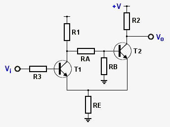 Suppose the input voltage Vi is close to zero. T1 has no base current, so it's off. T2 draws base current though R1 & RA, so it's on (and by design, it's saturated - that is, its collector-emitter voltage VCE is close to zero), so Vo sits at the mid-point of the potential divider formed by R2 & RE, somewhere between +V and ground.
Now suppose Vi starts to increase. T1's emitter voltage is held fixed by the current flowing in T2, so when Vi reaches about 0.6v above this value (call it VP), T1 will draw some base current and start to turn on.
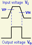
As it does so, T1 begins to starve T2 of base current, so T2 begins to turn off, and so its emitter voltage starts to fall. But this increases T1's base-emitter voltage, so T1 turns on more quickly. The positive feedback snaps the circuit into a state where T1 is on (and by design, saturated) and T2 is off. Vo now sits at close to +V.
Finally, suppose Vi starts to fall back towards zero. T1's emitter voltage now is controlled by its own emitter current. When Vi has fallen to about 0.6v above this value (call it VN), T1 will start to turn off. This allows T2 to begin to turn on again, adding its own emitter current to T1's and so nudging the emitter voltage upwards. This compels T1 to turn off more quickly, and once again positive feedback snaps the circuit into its other state, with T1 off and T2 on.
Thresholds and currents
I need to emphasize an important design constraint. Suppose Vi is rising slowly from zero, and reaches the threshold at which T1 switches on. This threshold (VP) is set by T2's emitter current flowing through RE. As soon as Vi reaches VP, T2 switches off, and the current though RE now comes via T1.
Suppose for a moment that this current is larger than that from T2. If it were, T1's emitter voltage would rise abruptly when T1 switched on. But T1 would then suddenly discover that its base voltage (Vi) was now smaller than its new emitter voltage, and would instantly switch off. But then its emitter voltage would drop again, and so it would turn on again. In other words, the circuit would oscillate.
It follows that the designer must ensure that the current in T1 (I1) is smaller than the current in T2 (I2), or the circuit won't work!
And it also follows that the threshold at which T2 switches on again (VN) must be lower than VP. The difference between the two thresholds is known as the circuit's 'hysteresis', by analogy with what happens in a transformer core, I suppose.
Design example
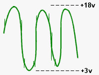 Design a circuit to digitise this noisy and distorted signal. Supply rails of +5v and +24v are available. The output signal must be compatible with digital logic operating at +5v.
A solution based on CMOS logic (eg. HC14) would be possible if the input signal could be scaled to suit the +5v rail. Using a comparator might be possible too, but the obvious approach here would be a transistor-based design using the +24v rail. I'd pick a couple of easily obtainable 30v npn switches - they're as common as apples.
Warning. What follows is not for those who insist on precision. Design need not always involve Difficult Sums!
The first step is to decide the threshold VP. From the waveform, it probably ought to be around 12 or 13v.
Next, choose the current that will flow in T2. A low value saves energy but implies a high value of collector load resistor, which might slow down the switching edges. Choose 3 mA in T2 for now. Then the emitter resistor RE will be [12v / 3mA] = 4k. Use 3.9kΩ. Next, calculate R2 as [(24v - 12v) / 3mA] = 4k. Use 3.9kΩ here too.
Finally, choose T1's collector current and hence the lower threshold voltage VN. The noise spikes look troublesome, so it would be sensible to aim for around 9 or 10v - which would give about 4v of hysteresis - which sets I1 at [9v / 3.9kΩ] = 2.3mA. Then R1 is [(24v - 9v) / 2.3mA] = 6.5k. Use 6.2kΩ.
R3 limits T1's maximum base current, which could safely be [2.3mA / 30] = 77μA (because the transistor won't have a current gain lower than 30), so R3 is [(24v - 9v) / 77μA] = 194k. Use 180kΩ. (I'm assuming that the circuit is driven from a zero-impedance voltage source. If it's not, then the source impedance can be subtracted from R3.)
That leaves RA & RB. RA is there to limit T2's base current when T1 is off, and RB ensures that temperature effects won't matter. The two resistors form a potential divider which must set T2's base at (say) 12.6v with T1 off, and draw a current significantly higher than T2's base current, which can't exceed [3mA / 30] = 100μA.
Choose the bleed current through RA & RB to be about 500μA, so that it's much larger than T2's base current.
Then if R1 were zero, the sum of RA & RB would be [24v / 0.5mA] = 48kΩ and with the divider mid-point at 12.6v, [RB / (RA+RB)] = [12.6v / 24v] = 0.53, which implies RB = 1.1 RA. This implies that RB is [48k x 1.1/2.1] = 25k and RA is [48k - 25k] = 23k. However R1 isn't zero, it's 6.2kΩ, so the real value of RA is [23k - 6k] = 17k. So, round the values down, since a bit more current won't matter, and choose RA = 15kΩ and RB = 22kΩ.
There. Finished. Now to build one and try it. Well, simulate it, anyway. It works as it's supposed to, switching at 12v and 8v.
Final circuit for the design example
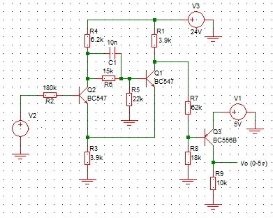
The output of this circuit swings from about 13v to 24v, whereas the spec says the output levels should be 0v and 5v. I need to add a level-shifting transistor powered from the +5v rail to correct this. The simplest solution is to add a pnp inverter.
And including a capacitor (of 4.7 or 10nF) across the 15kΩ resistor R6 (that is, RA) makes the circuit switch faster and more cleanly - the rise and fall times of the output edges are about 500 nsec.
The final circuit looks like this. I've ended up with 3 transistors and 9 resistors (and a capacitor). These 13 components would occupy an uncomfortably large area of PCB, and the assembly cost might raise eyebrows, too. There ought to be a better solution.
An alternative approach using three transistors
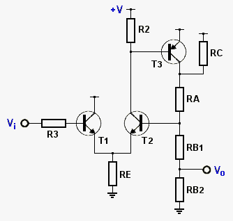 The original 2-transistor circuit is really just a long-tailed pair with positive feedback. Drawing it like that, and taking the feedback from a third (pnp) transistor T3 gives the circuit shown here. It works like the previous circuit, except that the pnp transistor's gain is now exploited rather more effectively.
It also uses fewer resistors - and one of those is only there to limit the output swing to the required 5v.
As before, when the input voltage Vi is close to zero, T1 has no base current, so it's off. T2 is on (short-circuiting RC), and so is T3. The output Vo is high.
As Vi rises, sooner or later it reaches a value sufficient for T1 to begin to turn on. This must happen when T1's base voltage slightly exceeds T2's. RA and RB form a potential divider that defines T2's base voltage, and these two resistors define the upper threshold VP.
When T1 turns on, it switches off T2 and T3. The output Vo drops to near zero (assuming RC is large enough).
Suppose now that Vi starts to fall. T1 will turn off again when its base voltage drops just below T2's. This voltage is fixed by the potential divider RC-RA-RB and can be set anywhere between zero (if RC=∞) and VP. One of the great advantages of this circuit is that both VP and VN are defined by potential dividers, as they would be in a solution based on comparators.
A simpler alternative
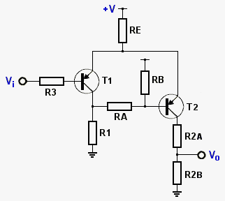 The original design solution was unnecessarily complex (13 components) because it solved the problem in two stages - first make a Schmitt trigger, then bolt on a level-shifter.
Combining these two stages into one involves nothing more complicated than replacing the npn transistors with pnp types. This solution uses just 9 components.
This circuit is (almost) exactly the same as the original, except that +24v and ground are swapped over. You might even say, Turn that Frown Upside Down! if you were one of those annoying people who insist on smiling all the time.
The output levels of +13v and +24v in the original circuit now become +11v and 0v. The spec calls for +5v and 0v, so I need only about half of the available output swing, which I can get by choosing suitable values for R2A and R2B.
An even simpler alternative
If you've read this far, you now know how the circuit works, how to design one, and how to tweak it. But you might still be wondering when, if ever, you would choose this approach.
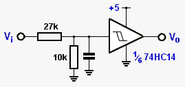 That is not an easy question. The answer depends on what kind of system you're designing. If the input signal is relatively large, and you decide that VP and VN must be far apart (to reject interference noise, for example), and the system already includes discrete components, a transistor-based solution might be the answer. If not, it might be worth trying a simple solution first, if only to see how well it works in practice. It's possible that the Design Example problem could be solved by the very simple circuit shown here (though actually, I doubt it).
References
Circuit consultant's casebook - TK Hemingway (Business Books, 1970)

