4: Second-order networks
In this chapter I discuss a couple of filters, which are really just frequency-dependent potential dividers. RC networks are widely used as filters. Later I show in detail how to design a bridged-tee notch filter.
Today op-amps can be cheaper than capacitors, so most analog filter designers routinely use op-amps to achieve the frequency response they want. There are many good textbooks on active filters, and I don't intend to cover the subject again here. Instead, I want to look more closely at how an engineer moves from analysing a general circuit to designing a particular circuit to solve a problem. Circuit analysis is usually easy - it's taught in schools, these days. Synthesis is harder. It involves understanding what the equations mean. I find that graphs help.
Low-pass filters


This circuit is a simple low-pass filter. Low-frequency signals applied to the input pass through unaffected, whilst high-frequency signals are attenuated by the capacitor. The network's transfer function - the ratio of output to input voltage (its Gain, if you like) - is:
G = vo/vi = 1 / (1 + jωCR) = 1 / (1 + jω/ω1)
where ω1 is evidently 1/CR, as I explained in Chapter 2.
There is a single down-break frequency, ω1. At frequencies higher than ω1, G begins to decrease (at 20 dB/decade) and the output signal's phase shifts steadily towards -90°. [And obviously, if the resistor and capacitor swap places, the network turns into a high-pass filter, but the principles I'm discussing stay the same, and it would be really boring to plod through the whole thing twice.]
Now suppose I add a second low-pass RC network, like this:

This two-stage network is just two single-stage networks joined together, so one might expect to see two down-break frequencies, one at 1/CR and the other at 1/D(R+S) [because for D, the potential divider includes both resistors] and a transfer function something like:
. . . 1 / (1 + jω/ω1)(1 + jω/ω2)
But that's not what happens.This circuit's transfer function is actually:
G = vo/vi = 1 / {1 + (jω)[CR + D(R+S)] + (jω)2CDRS}
and this expression does not readily factorise into two nice simple terms. Something more complicated is going on.

OK, let's build one and see what it does.
Choosing R = S = 10kΩ, and C = 100nF, D = 1nF (to make sure the break frequencies are noticeably far apart) gives the response shown in this graph. The voltage across C begins to roll off above the break frequency ω1, whilst the output across D shows two down-breaks, at ω1 and ω2, as expected.
The lower break-frequency (ω1), appears from the graph to be at about 160 Hz (that is, f1 = ω1/2π ≈ 160 Hz.) . This must be due to C, the bigger capacitor : the break frequency can be calculated as 1/2πCR = 159 Hz. The higher break-frequency (ω2 - where the response is 3dB down from where it would have been) shows f2 at about 16 kHz, and its value too can be calculated: 1/2πDS = 15.9 kHz. But I had expected that f2 would be given by 1/2πD(R+S), and it's evidently not.
And since I can clearly see two separate and predictable break frequencies, why won't the expression for G factorise into two separate break-frequency terms? What's going on?
The meaning of Q
The key to this puzzle lies in my original assumption that the break frequencies are far apart. They don't have to be. They could be identical. And if they are, what happens at the break frequency?

If I increase the value of capacitor D from 1nF to 50nF - so that the two break frequencies become (supposedly) the same - the network's response looks rather different.
Instead of two more-or-less distinct straight lines, the response now rolls off smoothly, and reaches its final slope of -40dB/decade by about 1 kHz. The network's response at low frequencies and high frequencies is much the same as it was before, but near the break frequency the shape of the response curve has changed.
It's actually quite useful to have a way of talking about this shape.

Engineers use the term Q as a label to describe the shape of the response at frequencies close to the break frequency.
The choice of the letter Q is not arbitrary. Originally, in the early days of radio ('wireless', back then), Q meant Quality. In particular, Q referred to the Quality of a coil. A high-Q coil (Q=100, say) had low inherent resistance, which allowed it to be tuned sharply and precisely. A low-Q coil (where Q=10 or less) was often useless.
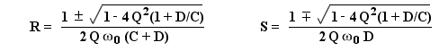
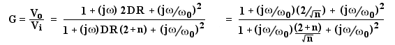
So applying this idea, it's possible - and sensible - to write a general expression for the transfer function of the second-order low-pass filter network like this:
G = vo/vi = 1 / {1 + (jω/ω0)(1/Q) + (jω/ω0)2}
The great advantage of this approach is that it focuses on what matters to the designer - the actual shape of the response. The design begins with a decision to choose particular values of ω0 and Q. Once they are settled, the component values can be found without worrying too much about the individual break frequencies.
Unfortunately, the circuit itself imposes a severe limit on the value of Q that can be achieved, and it's not impressive. The break frequencies ω1 and ω2 can be written in terms of ω0 as:
ω1 = ω0/k, and ω2 = kω0 . . . . . . so that ω1ω2 = ω02,
which means that Q = k / (1 + k2), and whilst k can be anything you like, most values of k make Q very small. (In the example above, when R=S=10kΩ, C=100nF and D=1nF, k is 10, and Q = 0.1.) In fact, it's not hard to prove that the maximum value Q can have in this circuit is 0.353, which happens when D=50nF. Higher values of Q can be achieved by active filters - that is, by circuits which include op-amps.
Calculating the component values
The transfer function G is expressed above in two forms - one involving C, D, R & S, the other using ω0 and Q - so finding the component values is a matter of mapping one equation onto the other. With four unknowns (C, D, R, S) and two fixed values (ω0, Q) the designer is free to choose two other values, and it's often convenient to pick sensible values for the capacitors (and by sensible I mean small preferred values, to keep the cost down). Assuming then that R & S are to be calculated, the expressions are:
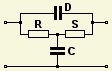
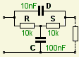
Bridged-tee notch filter
This circuit looks like a parallel combination of a low-pass filter (through R & C) and a high-pass filter (via D & S). Its response is dramatically different from either.
I'm going to use this simple circuit as a way of illustrating the design process, from analysing a circuit, to understanding what the equations mean, to designing the optimum solution to a problem.

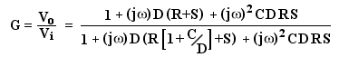
The first step is to analyse the circuit and find its transfer function:
To get a sense of what this expression means, consider what happens at the extremes of frequency.
At dc (that is, when ω = 0), G = 1. This means that the circuit behaves like a piece of wire - it doesn't alter the signals passing though it. The same is true at ω = ∞. How about when ω = 1/√(CDRS)?
At this special frequency, both (jω)2 terms become -1, so the expression simplifies to (R+S) / (R [1+C/D] + S)
which must be less than 1. How much less? If I write the capacitor size ratio (C/D) as n, and assume for a moment that
R = S, then at this special frequency (which I may as well label as the break frequency, ω0) G becomes

Gω0 = 2 / (2 + n)
In other words, only signals close to ω0 are attenuated. The circuit is a notch filter. Its task is to suppress a single interfering signal to make subsequent processing easier.

The depth of the notch depends crucially on the ratio of capacitor values. For a given value of C, a smaller D gives a deeper notch. The graph demonstrates what happens when C=100nF and R=S=10kΩ. For example, when (C/D) =10, the notch depth is (2/12) which translates to -15.6 dB.
But suppose the response shape you need is slightly different from any of these examples (and in practice it always is) ...
What does the transfer function equation actually mean?
To begin with, let's make the equation simpler. Once again I'm going to use the label n for the ratio (C/D), and I'm going to assume (for now) that R = S. Also, I'm going to write (jω)2CDRS as (jω/ω0)2. Then the equation becomes:
It's tempting at this point to write the equation in terms of Q, as I did for the low-pass filter. But the top and bottom expressions are slightly different, and each would have a different Q, so that wouldn't help much. It's clear from the graph above that there is a Q involved - indeed, it can be quite large - but should there be two of them? How do I sort out what these expressions mean?
Here's an idea: both the top and bottom are quadratic equations in (jω/ω0), and
The expression for y will factorise into real roots as long as b2 is greater than 4ac. If b2 is too small, the roots become complex.
So do the top and bottom expressions in G have real roots or complex ones? It shouldn't be hard to find out. For the top expression, the roots are real if n < 1 and for the bottom, the roots are real for any value of n. In other words, the top expression never has real roots (because n < 1 means there won't be a notch), and the bottom one always does. So G can be written as:
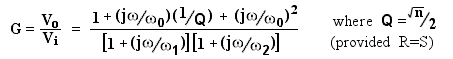
This is much easier to interpret. The top term is a second-order upbreak, with a Q at ω0 that could be significant if (C/D) is large. The term on the bottom is two first-order downbreaks. The overall response is a combination of these two shapes and, as I showed in Chapter 2, by thinking of the magnitudes of the expressions in log terms (that is, in dB), the overall response |G| is simply the difference between the top and bottom terms, since
log |G| = log |top| - log |bottom|

There are two small difficulties - I don't yet know where ω1 and ω2 are, and I don't know the shape of the top expression. However, it's not difficult to show that ω1 and ω2 are located symmetrically on either side of ω0. In fact, I could write them as
ω1 = kω0 . . . & . . . ω2 = ω0/k . . . so that ω1ω2 = ω02 . . . where k = (2 + n ± √[4 + n2]) / (2 √n)
It seems that ω1 and ω2 spread apart quite rapidly as the notch depth increases. This means that the price of eliminating a single interfering signal is that a wide range of signals close to that frequency are attenuated too. There are no free lunches.
Turning now to the top expression, its magnitude is:
|top| = √[ 1 + (ω/ω0)2[(1/Q2) -2] + (ω/ω0)4 ] . . . . which is easily evaluated with a spreadsheet (here, for Q=10) as:
 shows a sharp peak at the break frequency")
| ω/ω0 | |top| (dB) |
| 0.1 | -0.09 |
| 0.2 | -0.35 |
| 0.5 | -2.5 |
| 1 | -20 |
| 2 | +9.6 |
| 5 | +28 |
| 10 | +40 |
| 20 | +52 |
| 50 | +68 |
| 100 | +80 |
So now we know the shapes of the responses, it's straightforward to combine them and see what the overall response looks like.

Is there anything to be gained by giving R and S different values?

Suppose that I write (S/R) = a (where now a is no longer necessarily 1) as well as (C/D) = n. The expressions do get a bit more complicated, but it's worth making the effort because this points the way towards achieving a better notch. The graph shows what happens when S is made much larger than R. (I have adjusted the capacitor values to give the same resonant frequency and notch depth.)
The useful equations are the ones concerning notch depth, and k (the ratio ω0/ω1).
Notch depth now is Gω0 = (1 + a) / (1 + a + n)
and k, which sets the shape of the notch (that is, the steepness of the slope), is

Now, I would like to design a filter in which the notch is as deep as possible (that is, Gω0 is large) with sides sloping as steeply as possible (that is, k is small) and it turns out from these equations that it can't be done.
The notch is deepest when a is small, but the slope is steepest when a is large - specifically, when a = n. Here is the graph showing what happens when n = (C/D) = 20. Any design must be a compromise.
 will not give a steep-sided deep notch")
Sketching the equations in terms of n instead of a makes the point even more starkly. To achieve a modest notch depth of 20 dB is not straightforward if the notch sides must slope steeply.
So although this circuit can deliver a deep notch, signals at frequencies some distance away from the notch will not escape unscathed. If the notch is to be at 100 kHz (say), then allowing k=5 (say) would mean that frequencies between 20 kHz and 500 kHz are attenuated too.
What happens in the real world when a load resistor is connected across the output terminals?

The network is bound to have some sort of load connected, but it's not really worth flogging through the equations again. Provided the load is substantially larger than S, nothing much happens to the response.
I show here the effects of connecting load resistors of various sizes. The output is reduced at low frequencies, but high-frequency signals find their way to earth through S and C just as they did before.
Design example:

Design a filter to attenuate a 44 kHz signal by at least 12 dB.

The graph above of Gω0 against n shows that even with a 1 dB tolerance margin added to the notch depth, I could still achieve steep sides.
A 13 dB notch means:
Gω0 = (1 + a) / (1 + a + n) = -13 dB = 0.224, so now I must choose a or n and then calculate the other one. Try choosing n=470 (to give the capacitors standard values) : then a=134 (and so k=1.88). The notch is to be at 44 kHz, so
ω0 = 1/ √CDRS = 2 π 44E3 = 1/ DR √(a n) = 1/ 251 DR, so DR = 1.44E-8
Now choose the smaller capacitor. Make D = 100pF, so then C = 47nF. So R = 144Ω, and so S = 19.3kΩ. There. Done. A quick simulation shows I've met the spec.
The resistor values are non-standard though. What happens if I use preferred values of 150Ω and 20kΩ? Not much - it still meets the spec. Check quickly on the simulator that 1% resistors and 5% capacitors would do : yes, still plenty of margin. I'm confident that this network would pass production testing. The great strength of the bridged-tee filter is that it works as designed, without any need for precision components or manual trimming.